PCB Design
Overview
This section covers the process of taking your crossover circuit from the simulation phase and turning it into a physical Printed Circuit Board (PCB). While you can solder components point-to-point, creating a custom PCB makes the final build reliable, clean, and much easier to assemble inside the shell.
For the actual PCB design, we will be using KiCad. This guide focuses specifically on the workflow for designing IEM Crossovers. If you are new to KiCad, I highly recommend watching these tutorials to understand the interface before moving forward:
Creating the Schematic
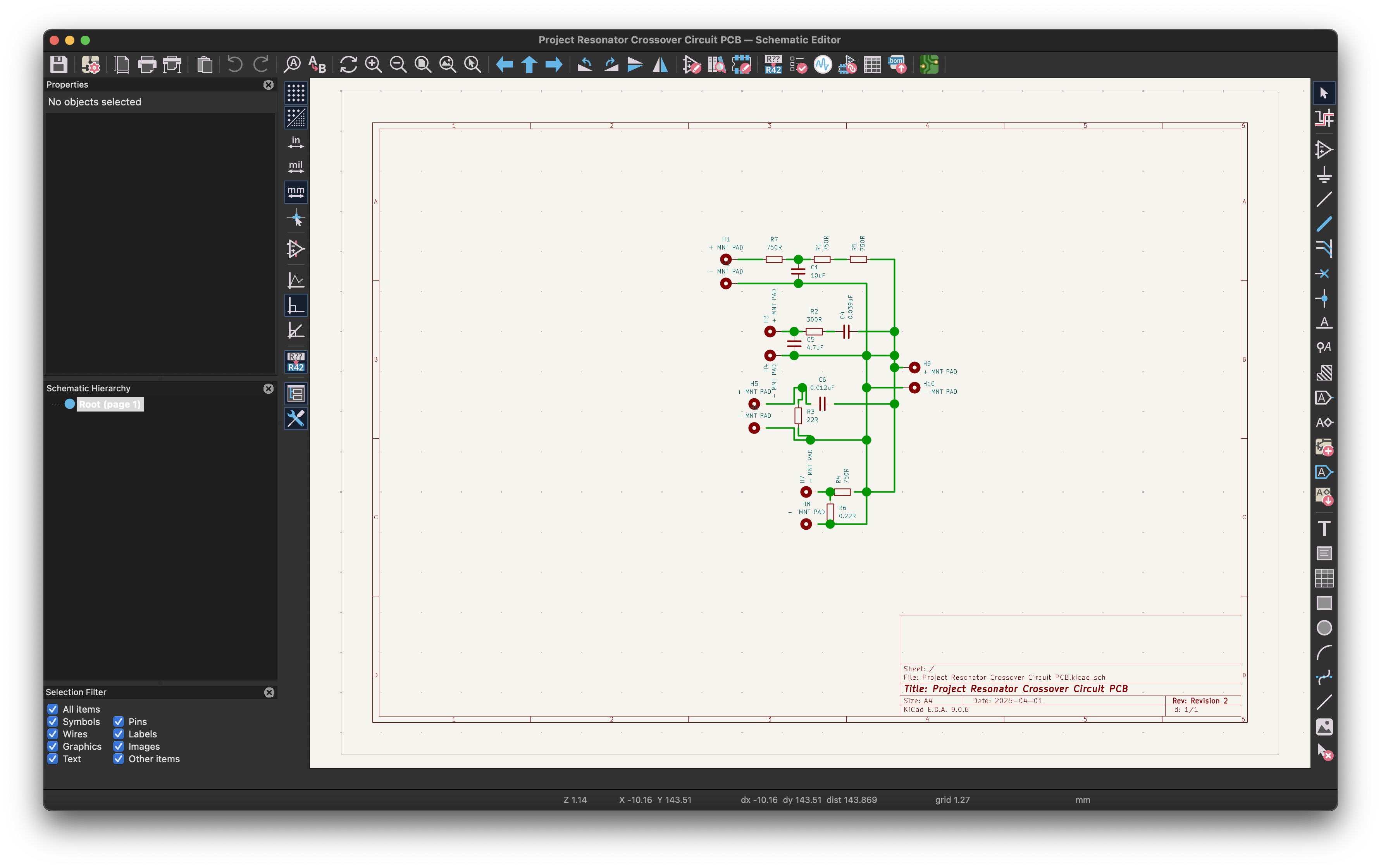
The first step is translating your VituixCAD simulation into a schematic that KiCad can understand. In a simulation, you have specific driver blocks, but KiCad doesn't need to know what the driver is—it only needs to know where the electricity goes. Since we can't download specific "driver symbols," we use Solder Pads (often called Test Points) to represent these connections. You will simply place two pads for each driver (one positive, one negative) and two pads for your input socket.
The wiring logic for IEM crossovers is almost always a parallel network. This means you will connect the start of every filter branch (Woofer, Mid, Tweeter) to a single Input + pad. From there, the components for each driver are wired in series, exactly as they appear in your simulation diagram.
Grounding requires a specific strategy in the schematic. You must connect the negative side of every driver and every parallel component to a single GND symbol. This tells the software that all these points share a common return path. Even though they look like separate connections in the schematic view, this logic allows us to later connect them all automatically using a ground plane or shared traces.
Defining the Board Shape
A standard square PCB won't fit efficiently inside an organic shell shape. To get the best use of space, we design the board outline to match the internal cross-section of our shell using Fusion 360 (or your preferred CAD software).
Start by creating a sketch on the plane where the crossover will sit. Project the internal walls of the shell onto your sketch, and then use the Offset tool to bring that outline inwards by 0.2mm - 0.4mm. This offset is critical; if the PCB is the exact size of the shell interior, manufacturing tolerances or resin shrinkage might make it impossible to fit, or inserting it could crack the shell. Once the sketch is ready, export it as a .dxf file and import it into KiCad on the Edge.Cuts layer.
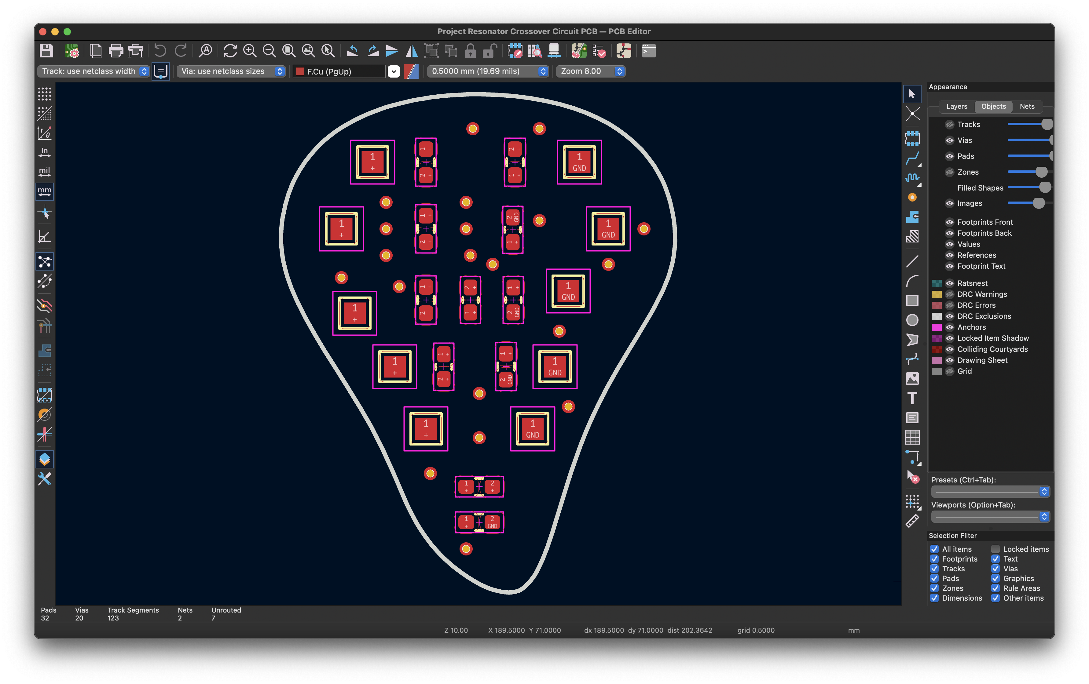
Component Placement
With the board shape defined, the next task is to fit the components inside the outline. Your goal is simply to move, rotate, and adjust the components until they fit cleanly within the space.
Try to place components that are connected in the schematic physically next to each other on the board. Shorter distances mean less resistance and less chance for interference to be picked up by the track. If you plan to route traces on the back of the board to save space, remember to leave small gaps between components to fit Vias (the holes that connect the top and bottom layers).
Signal Routing
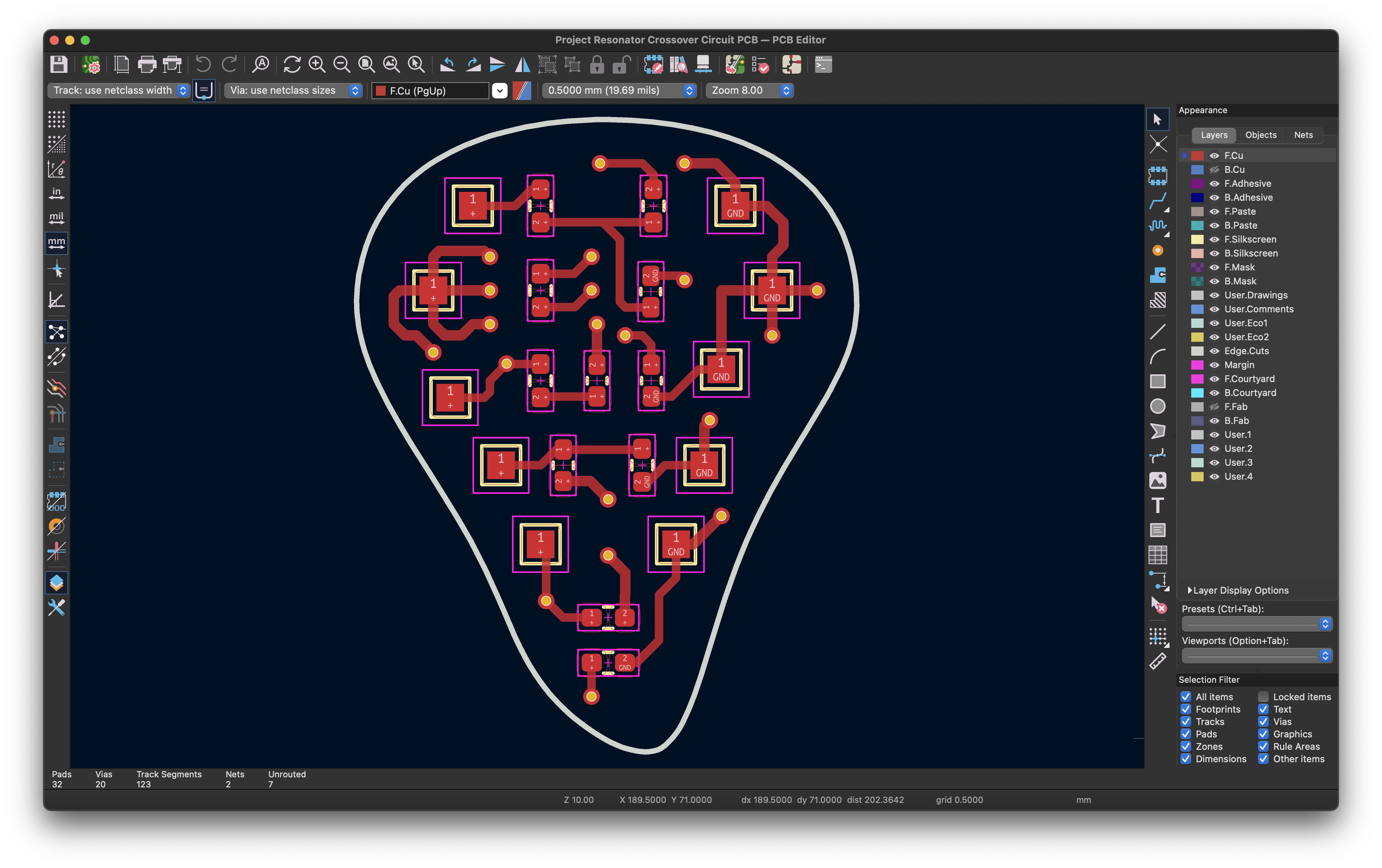
Once the components are placed, you need to connect the pads using copper traces. We usually route "Signal" (+) on the Top Layer (Red).
A good baseline width for these signal traces is 0.25mm. This is a safe middle ground—wide enough to be durable and carry the low current of an IEM without issues, but thin enough to navigate between tight component pads. If you have extra space, you can increase the width (e.g., to 0.4mm) to further reduce electrical resistance (R = ρL/A), which is always beneficial for audio. Conversely, you can drop to 0.15mm or 0.2mm if you need to squeeze through a tight spot, though these thinner traces are more fragile.
When drawing these paths, avoid sharp 90-degree corners. Instead, use two 45-degree turns to make a corner. While modern manufacturing can handle 90-degree turns without creating "acid traps," the 45-degree standard is structurally more robust and professional.
Ground Routing
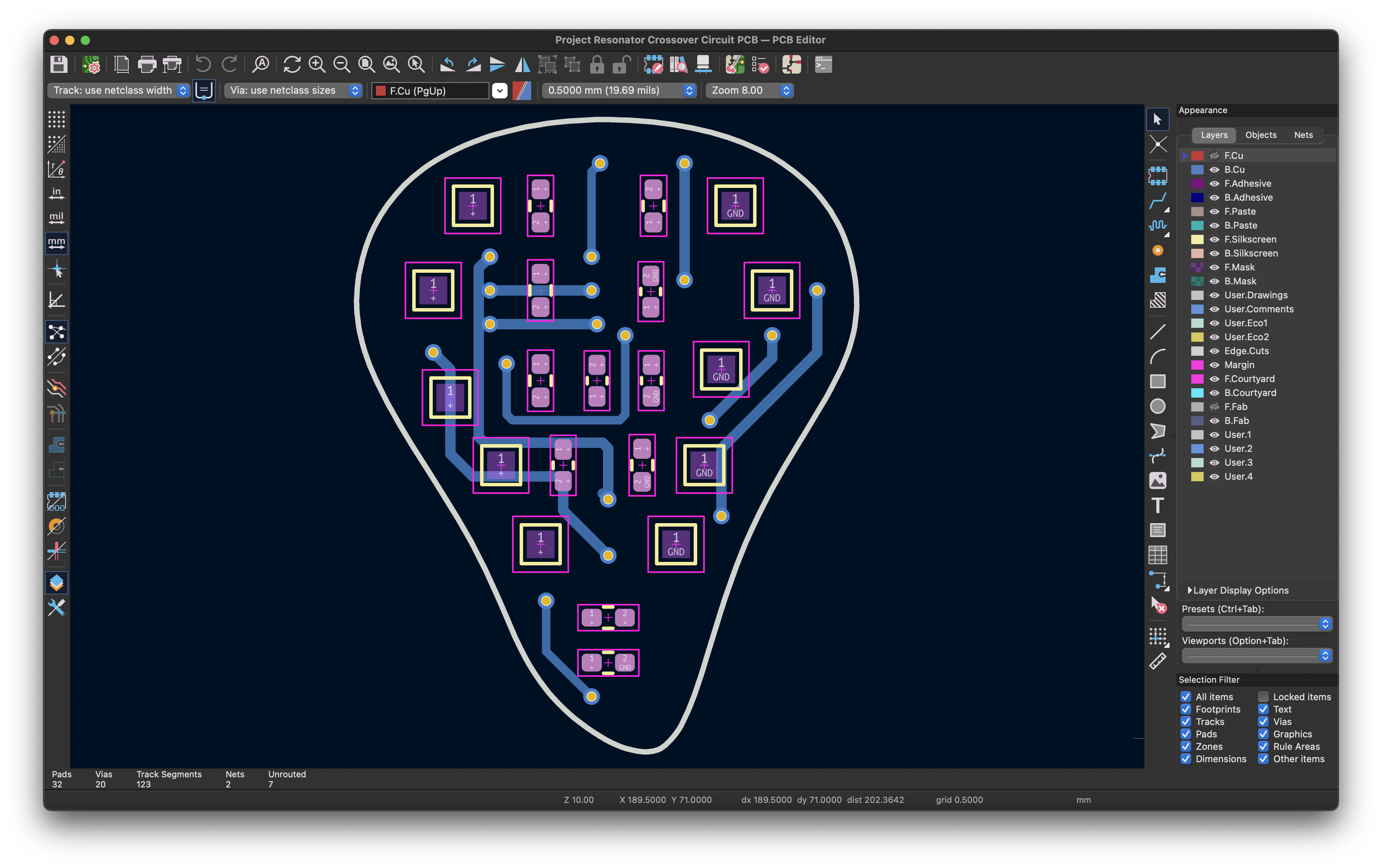
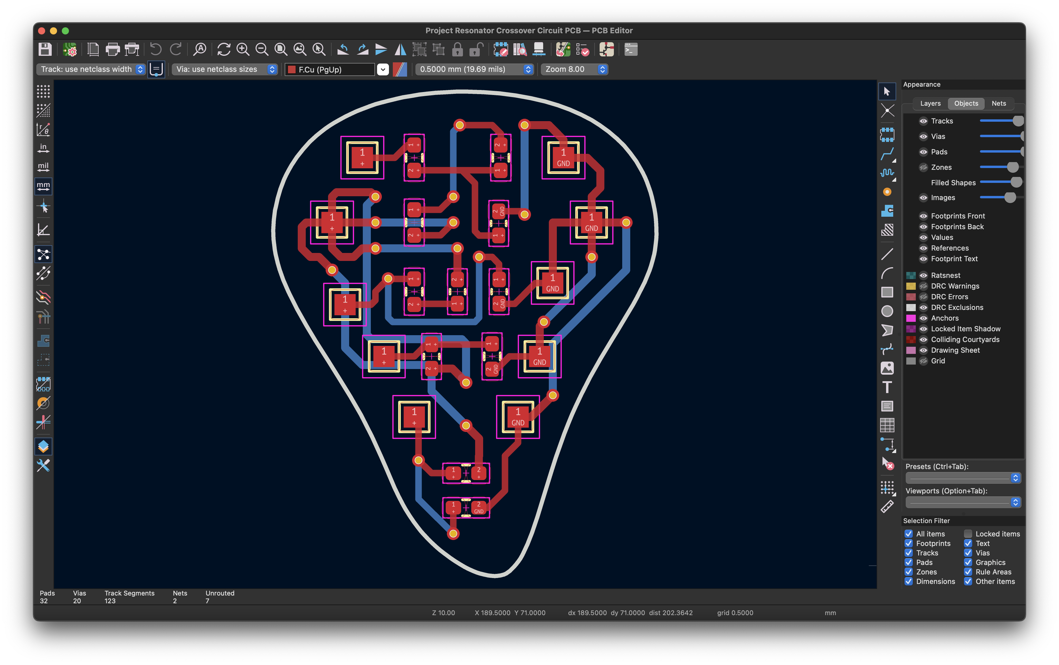
For the return path (Ground), the top layer is often too crowded to route everything cleanly. The most effective strategy is to place a Via next to your component's ground pad to drop the connection to the Bottom Layer (Blue).
This allows you to route the ground traces underneath your other components without collisions. You can see this in the image below, where the blue traces on the back layer eventually meet up at the large Global Ground pad (the pad with the "plus" shape of vias).
 This is what the final routing looks like:
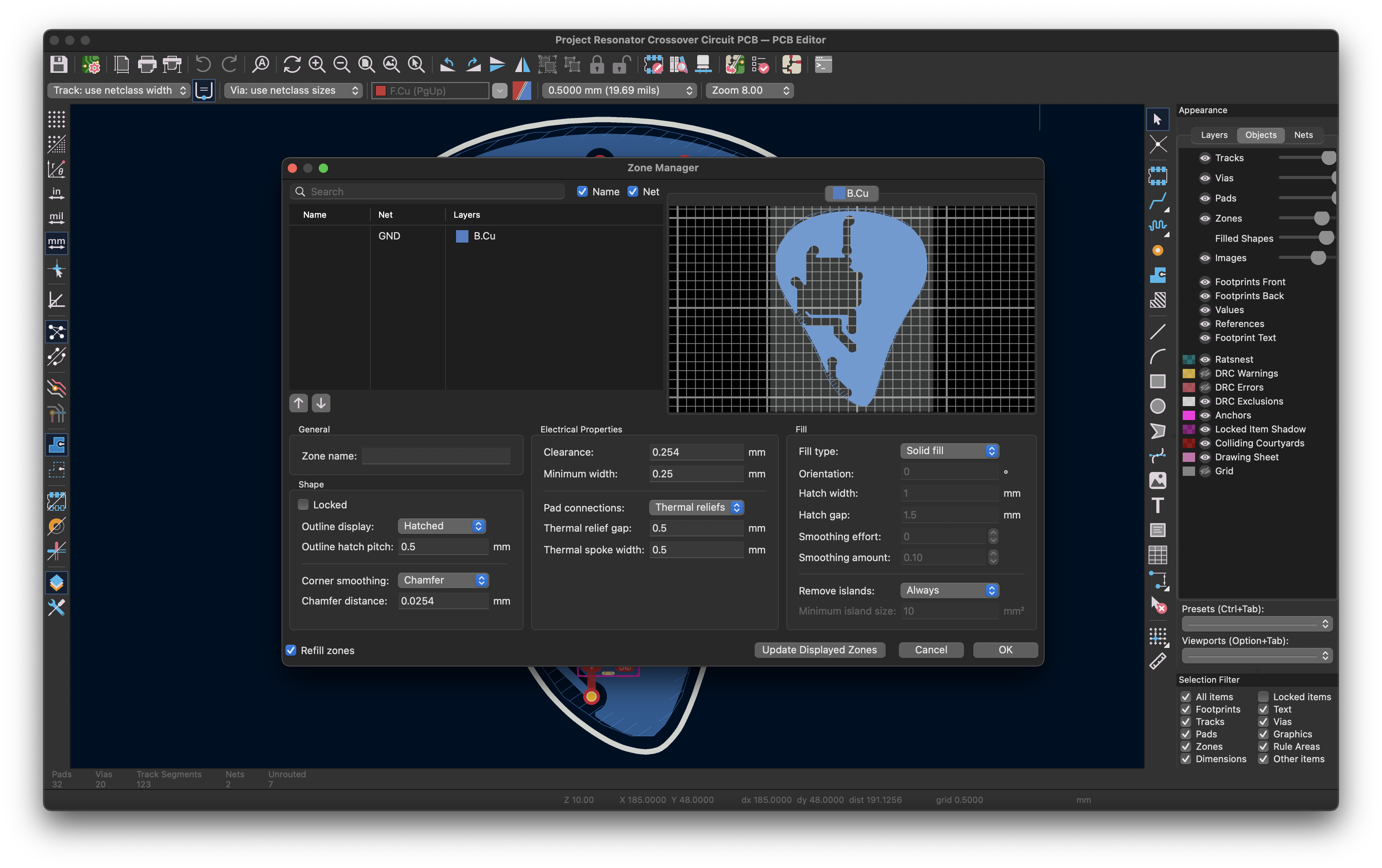
The Copper Pour (Ground Plane)
To finish the design, we use a Copper Pour (Filled Zone). This floods any unused space on the board with copper and connects it to the GND network. This effectively turns your ground routing into a giant, low-resistance shield that protects your signal from interference.
When connecting small component pads to this large copper plane, soldering can become difficult because the copper sucks the heat away from your iron. To prevent this, we use Thermal Reliefs. These are small "spokes" that connect the pad to the plane rather than a solid connection.
In KiCad's Zone Manager, you should verify your settings for these reliefs. A Relief Gap (the air gap between the pad and the copper) of 0.25mm to 0.3mm is standard to prevent solder bridging. The Spoke Width should be around 0.25mm to 0.4mm—thick enough to carry current, but thin enough to limit heat transfer during soldering.
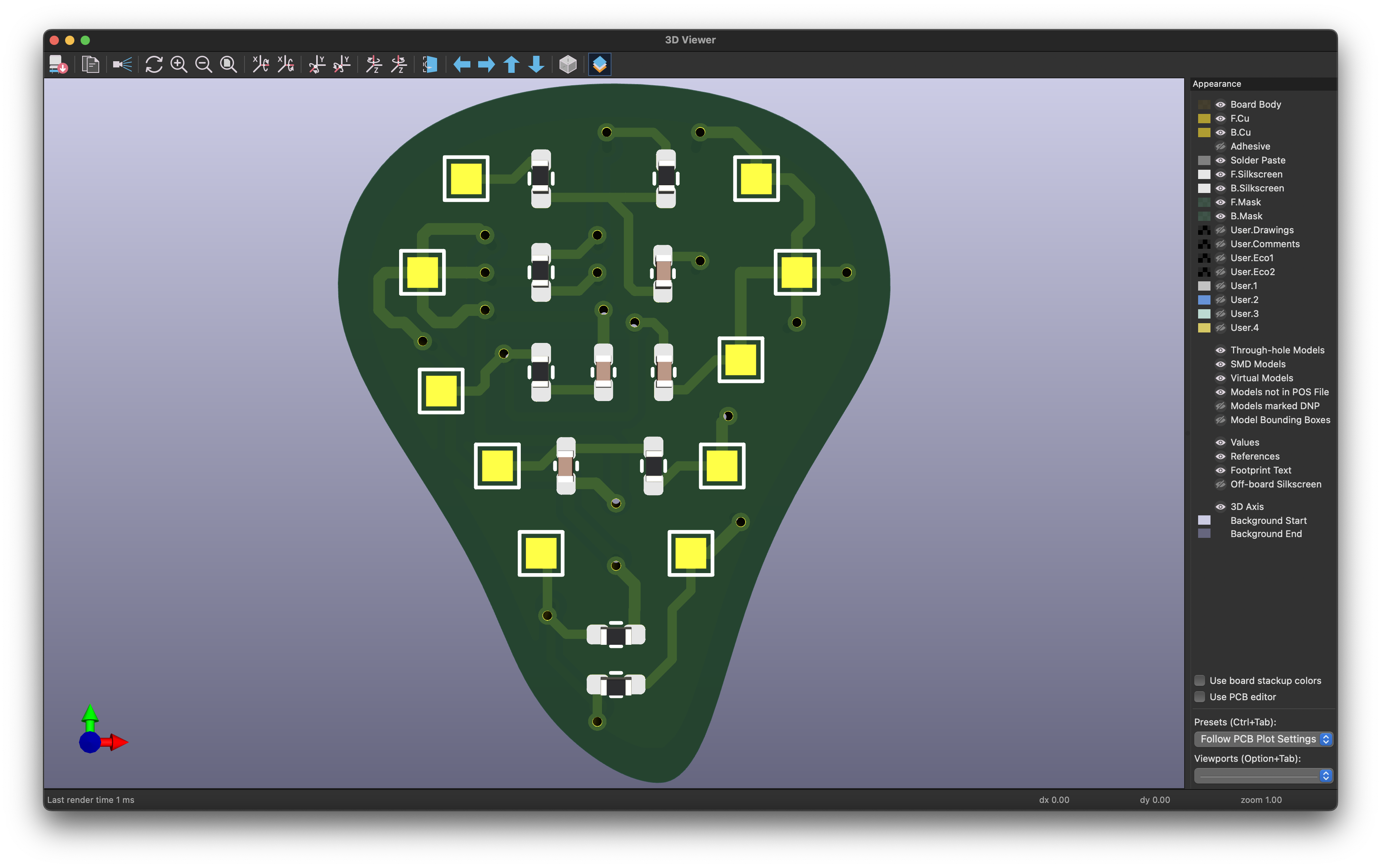
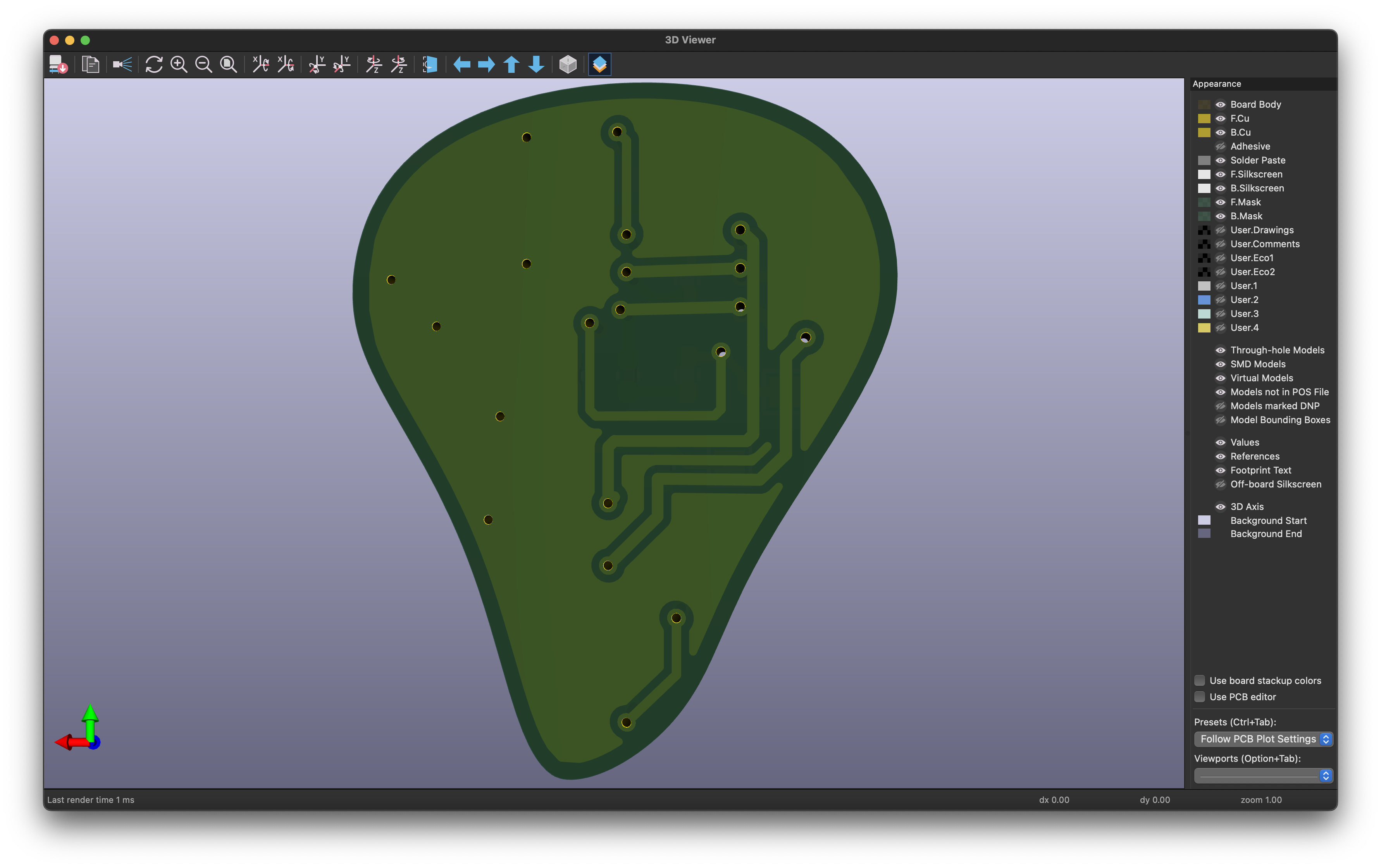
Visual Verification
Before exporting, press Alt+3 to open the 3D Viewer. This allows you to inspect the board for errors like components hanging off the edge, blocked input pads, or misplaced vias.
Front Side (Components & Signal):
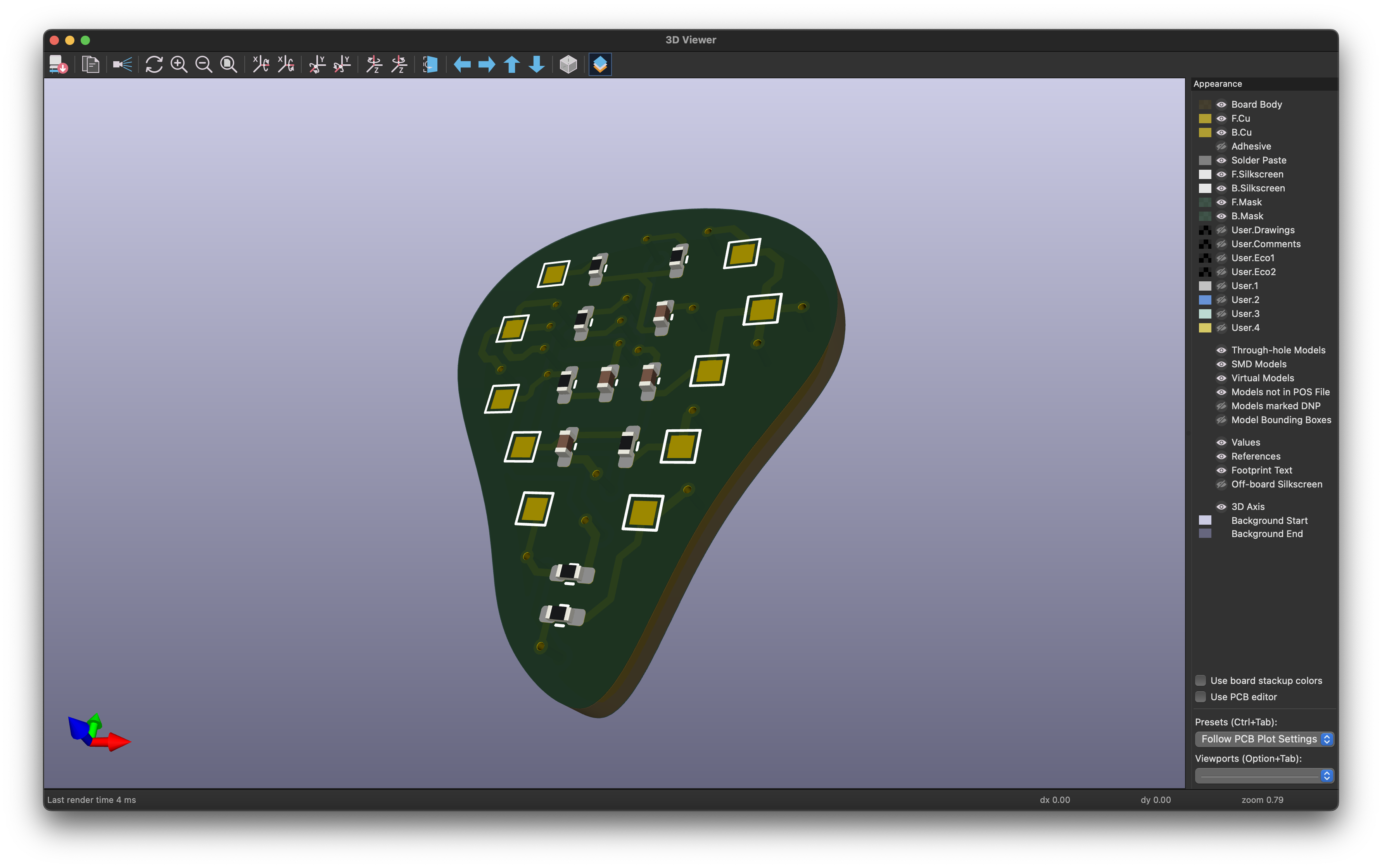 Back Side (Ground):
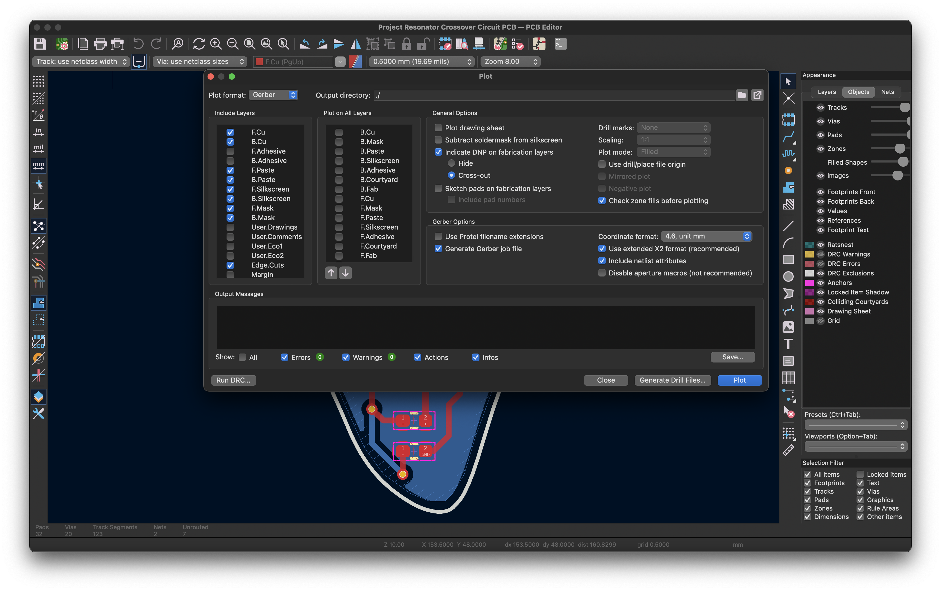
Manufacturing (Gerber Files)
We send Gerber Files to the manufacturer. These tell the machines where to print copper, solder mask, and drill holes.
To generate them, go to File > Plot and select the necessary layers (F.Cu, B.Cu, Masks, Silkscreens, and Edge.Cuts). Crucially, you must also click "Generate Drill Files," or the manufacturer won't know where to drill your vias. Zip all the generated files into a single folder to upload to your manufacturer of choice (like JLCPCB or PCBWay).
Citations & Further Viewing
- "KiCad Tutorial 6 - Schematic Capture," YouTube, https://www.youtube.com/watch?v=ESnDQl7ZM5o&list=PL4ahDGGN5zBFhmGqVUoBdOnjuF_9HXV5L&index=6 (accessed Dec. 28, 2025).
- "KiCad Tutorial 7 - PCB Layout," YouTube, https://www.youtube.com/watch?v=3FGNw28xBr0&list=PL4ahDGGN5zBFhmGqVUoBdOnjuF_9HXV5L&index=7 (accessed Dec. 28, 2025).
- "KiCad Tutorial 8 - Gerber Files," YouTube, https://www.youtube.com/watch?v=AuBZ1W80c9s&list=PL4ahDGGN5zBFhmGqVUoBdOnjuF_9HXV5L&index=8 (accessed Dec. 28, 2025).